UPNOD 1: Reverse engineering a vintage TelCo card.
Posted on by Idorobots
Since my last actual post on this blog I have acquired a new class of hobbies - electronics. Most recently, reverse engineering of really old computers. This series of posts will be about a vintage eighties TelCo computer-card-thing marked UPNOD CARD0117 TN64 I bought on a local auction:
All my findings will be posted on this blog and the accompanying data will be gathered in this GitHub repository.
From what I was told, the card came from an old internal telephony system of the Mechanics Department of the Tadeusz Kościuszko University of Technology. More precisely, it was one of the backup boards for said system and the guy insisted it was in mint condition and hasn't been used (not quite true, more on that below). They apparently modernized their internal systems (about damn time if you ask me) and trashed whole racks of similar electronics saving only this one card, because it was clean.
Board
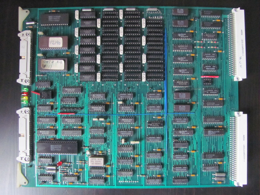
The card uses an SGS-made Z80 microprocessor, an SGS-made Z8430 programmable timer chip, whoppin' 64 KB of dynamic RAM, 16 KB of ROM and a bunch of electronics voodoo all over the place. It almost resembles a generic Z80-based microcomputer if not for the discrete implementation of IO devices next to the DIN41612 connectors (more on that later in the series). The board has two layers, with single-sided load and appears to have been auto-routed. There are multiple test point headers on the board making it easier to test it if I ever run it and find a way to make it do anything. It's marked TN64 on the PCB and TN104 on one of the connectors - I assume TN64 is the PCB layout, and the actual model number is determined by both the layout and the loaded software.
What's pretty neat about this board is the abundance of blue mod-wires - the board has been upgraded at least once in the past (so it can't be "new old stock" as the guy I bought it form has claimed), possibly twice or upgraded once and then scavenged for parts later (there's one 10-pin SIP package desoldered, one 8-pin DIP package missing & one RAM stand badly damaged). All the reverse-engineered schematics you'll find in this series & in the GitHub repository will follow both the original layout (TN104) and the modded one (marked TN135 with a faint marker).
Software
There are two 8 KB EPROMs on the board - the top one marked v2196 and the bottom one marked ONT0 RIB (0:1). The bottom ROM is dedicated to program memory only while the top one contains all kinds of UI strings in what appears to be Norwegian:
< NDH - UPNOD TCS-2000 terminal-veksler >
< Velg datamaskin/system ?  ( ? gir hjelp ) >
< Datamaskin/system ? >
< Forbindelsen nedkoblet >
LOG OG UD
< Alle porter med |nsket hastighet er opptatt >
< Feil valg, ? gir hjelp >
< Ikke tillat valg, ? gir hjelp >
< Valgmulighet:
    N,A = ND500.182
    D,A = Discovery System A  (DSA)
    ...............................
 \nsker de ytterligere hjelp,skriv H >
Kontroll-sekvenser i Upnod TCS 2000:
  1. N}r datamaskin velges:
     -Tastes <CTRL+C> f|r <CR> vil brukeren f} tildelt en
      datamaskinport med lavere hastighet enn terminalens.
      Denne mulighet kan brukes n}r alle datamaskinporter
      med |nsket hastighet er opptatt
     -Tastes <CTRL+D> f|r <CR> sl}s lokalekko av.
     -Tastes <CTRL+E> f|r CR sl}s lokalekko p}.
     -Tastes <ESC> istedet for <CR> sl}r du
      p} XON/XOFF flytkontroll
  2. N}r du er oppkoplet
     -Tastes <BREAK> etterfulgt av <CTRL+X> kan en av
      f|lgende kommandoer benyttes:
      <CTRL+A>: sl}r p} XON/XOFF flytkontroll.
      <CTRL+B>: sl}r av XON/XOFF flytkontroll.
      <CTRL+D>: sl}r av lokalekko.
      <CTRL+D>: sl}r p} lokalekko.
      <CTRL+F>: medf|rer at UPNOD TCS-2000 kopler ned
      linjen mot datamaskinen. NB!! Du kan fortsatt v{re
      logget inn p} datamaskinen.
There are also some English strings present:
*** Illegal command
*** Not computerport
*** Nonexist. group
*** Illegal priority
*** Not local port
*** No ports
*** Port connected
, Remote comm
*** Invalid porttype ***
*** Not connected ***
Computer:
*** Illegal address
*** No free buffers
*** No message
**** Port connected ***
Some of them are quite amusing:
Illegal error
THE QUICK BROWN BOX JUMPS OVER THE LAZY FROG
Yeah, you don't want to get an Illegal error, do you?
Judging by the contents of the ROMs and by what the guy I bought this card from said, I can quite confidently say that this card was a Norwegian TelCo terminal controller for some remote devices. It allowed the operator to open new ports and map them to internal RAM buffers (more on that in a later post) and in general was a pretty complicated machine for 16KB of program memory & 64KB of RAM.
Enough of the words, let's see some reverse-engineering!
Starting with the clock circuit roughly located here on the board:
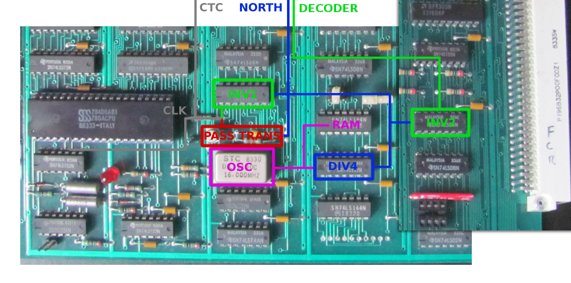
...which translates to:
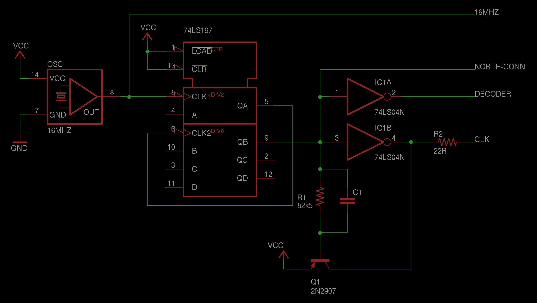
The 16 MHz oscillator signal (magenta) is divided by 4 (blue) to obtain the main CLK frequency of 4 MHz which is later inverted (green). The weird thing is, that the clock circuit's components are mostly located right next to the oscillator & the microprocessor except for one of the inverters which has been placed all the way on the other side of the board with the clock signal traveling all the way there and back with lot's of space for interference. Also, there's a curious pass transistor circuit (red) across one of the inverters going to the Z80 and the CTC. Based on its placement and the RC network at its base I speculate it's there either for waveform shaping or to give some extra current handling capability to the inverter feeding Z80 CLK pin. Or both. It's pretty baffling, though.
¯\_(ツ)_/¯
After some hand-wavey simulations using the Falstad circuit simulator the waveform shaping hypothesis seems plausible. After taking inverter output capacitance & impedance into account (disregard the ridiculous 10 uF value, it's there to compensate for low frequency of the simulated clock signal) and fiddling with RC circuits parameters I came up with this:
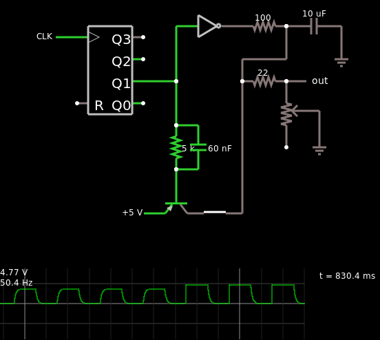
The initial four cycles were captured with the pass transistor switched out of the circuit. As can be expected, the waveform is far from a perfect square wave and may cause trouble when applied as the clock signal. When the pass transistor is enabled however, the initial rising edge is far sharper as exhibited by the last three cycles of the simulated waveform. Sounds reasonable enough for the girls I go out with and according to some sources:
The CPU samples the data from the memory on the data bus with the rising edge of the clock of state T3 and this same edge is used by the CPU to turn off the /RD and /MREQ signals.
Other than that, the 4 MHz clock signal as well as the unmodified 16 MHz oscillator signal go off to the RAM circuit and the PATA-style connector next to the ROMs I dubbed North.
More reverse-engineering shenanigans to come...
2016-03-02: Updated clock circuit placement diagram & description. 2016-03-08: Updated clock circuit schematic & placement diagram.