UPNOD 2: The reset circuit.
Posted on by Idorobots
A second installment in the UPNOD series, this time we'll take a look into the reset circuitry of the telco card.
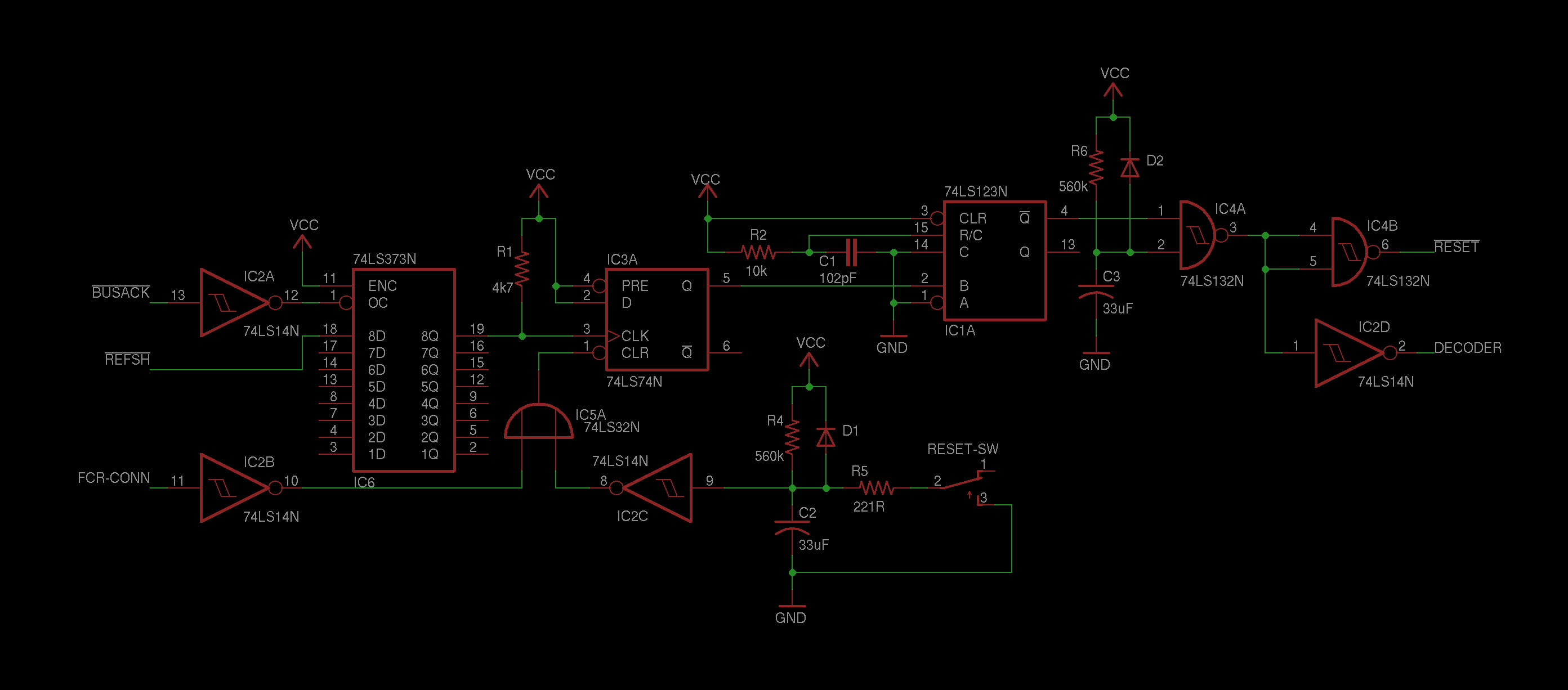
As the title implies, this circuit is responsible for generating a proper Z80' reset sequence. Z80, being a rather dumb piece of clever electronics, may boot up in an undesirable undefined state and requires a few cycles of special treatment to properly initialize internal register values. This circuit does just that - it generates the initial reset pulse and handles reset signals coming from other parts of the board, all while maintaining proper synchronization.
When the board first boots the 33uF C3 by the 74LS132 Schmitt trigger NAND ensures that one of the NAND inputs is held low for a certain time making it constantly output a logical high, and in turn a logical low on the RESET line that goes straight to the Z80 causing a reset sequence. Similarly, 33uF C2 capacitor by the reset switch ensures that the input of the 74LS14 Schmitt trigger inverter is held low, in turn, ensuring that the 74LS74 flip-flop is NOT reset. Once both C2 and C3 charge, the Z80 is assumed to be properly initialized, and the 74LS132 NAND turns into an inverter and operates as such forwards. The Q output of the 74LS74 flip-flop is initially undefined, but once the initial reset pulse ends the flip-flop itself is put into a reset state by holding its CLR line low forcing the Q output low. This ensures that the 74LS123 multivibrator configured as a one-shot trigger does NOT trigger and doesn't produce a pulse triggering Z80' RESET line to go low. Pressing the reset switch or pulsing one of the FCR-connector inputs disables the 74LS74 flip-flop CLR line by holding it high, causing a logical high value to be written to its Q output whenever its CLK line transitions from logical low to a logical high. This happens only, when the Z80 performs an instruction fetch and begins to refresh the memory while executing the opcode - the REFSH line goes high and triggers the flip-flop. That in turn triggers the multivibrator producing a new reset pulse for the Z80.
In sounds overly complex but that's due to the synchronous nature of this circuits operation. Here's how it looks on the PCB:
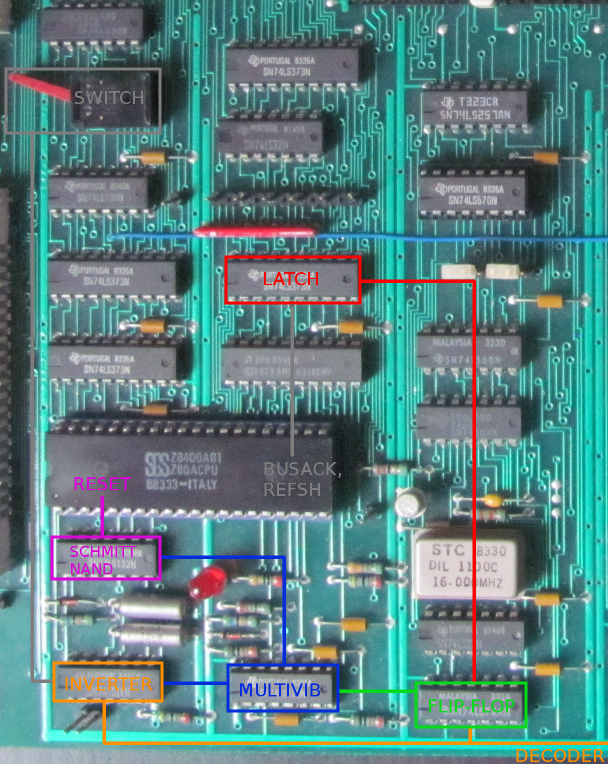
The circuit is placed rather neatly on the board with the only issue being the hardware switch, which is quite hard to reach assuming this board was just one of many telco boards of similar size all enclosed in a rack with little to no space between them. I guess you don't want to reset these things all that often.
Simulation
To validate my reverse-engineering attempts I figured it would be nice to simulate parts of the card, and to do that why not to use VHDL, right? Right!? I won't bore you with the gory details, but I've created a repository containing all the VHDL models along with some simulation results. To run the simulations yourself just navigate your favorite terminal emulator to the vhdl/ directory and run:
$ TARGET=target make view
...where target names one of the VHDL testbenches in the src/ directory. The Makefile assumes you have GHDL and gtkWave installed.
Here's a top level entity representing the entire reset circuit:
entity reset is
  generic (
    PULSE_WIDTH : time;
    ENABLE_DELAY : time
    );
  port (
    refsh : in std_logic;
    sw_pulse : in std_logic;
    fcr_pulse : in std_logic;
    reset : out std_logic
    );
end entity;
It accepts a REFSH line coming from the Z80 mock model along with the FCR-connector line and a switch pulse inputs. It outputs directly to the Z80 RESET line. The entity is built using smaller components, each modeling a discrete chip or a logical part of a discrete 74XX series chip. It's worth to mention, that VHDL does not allow simulating analog circuits, so instead I've added configurable time delays where applicable (for instance ENABLE_DELAY above). Here are some simulation results:
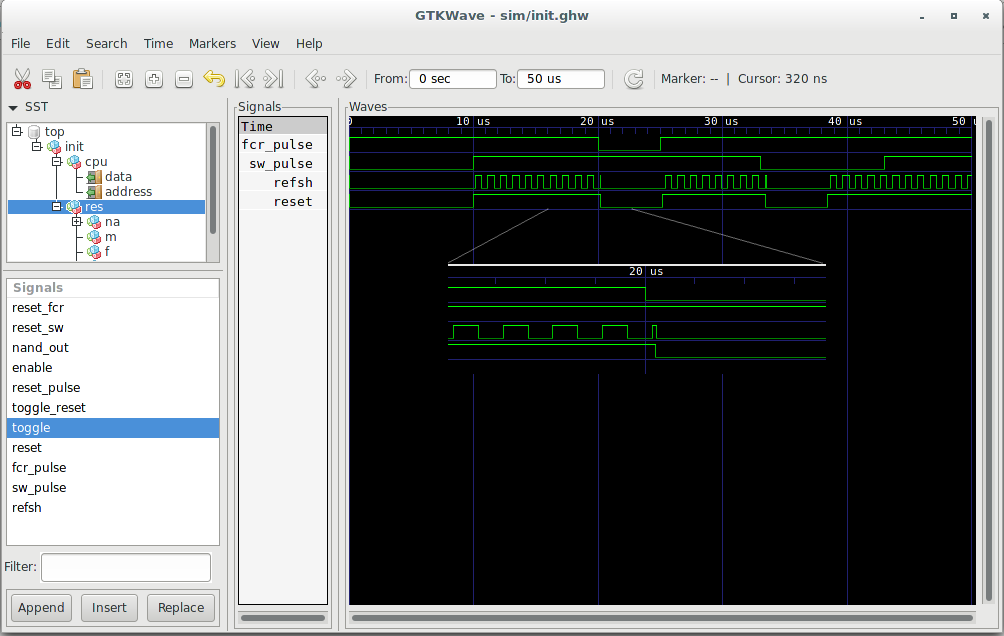
As can be seen, the model works pretty much as expected, initially performing a long reset pulse and then uniform pulses, synchronized to the positive edge transition of the REFSH line, whenever either FCR-connector line or the reset switch is triggered.
Action!
...but let's not rely only on models and simulations and actually see this stuff in action! Starting with the initial reset delay circuit:
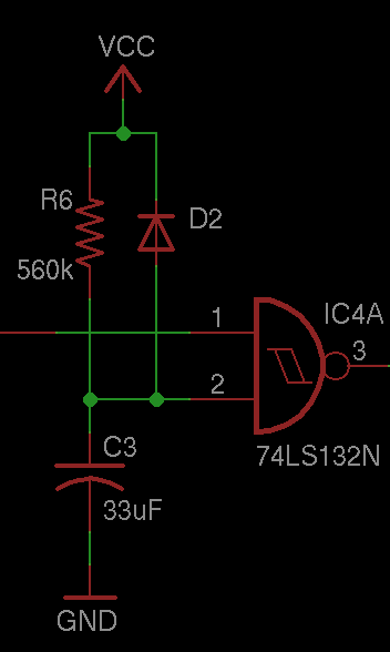
Here are some measurements:

The first channel (yellow trace) shows the voltage on the positive lead of the capacitor, the second channel (cyan trace) is the output of the 74LS132 Schmitt trigger NAND and the third channel (magenta trace) shows the other input of the NAND, which I emulated using a tactile switch and a (not quite) steady hand. As predicted, initially the NAND outputs a constant high state, but once the capacitor is charged to a threshold value of around 1.7 Volts it starts working as an inverter. Keen eyed readers probably noticed that I used different capacitance and resistance values as the capacitor charge curve looks off - I simply did not have any 560k resistors. This means that we can't measure the actual delay, but y'know, I'm pretty sure a few seconds is long enough for the Z80 to initialize.
Now, for the fun part, let's look closer at the entire reset circuit with a slight modification - instead of a Z80 I'm going to use a 6502. Right now, I only have a single Z80 CPU, and I'm not very keen on frying it on a breadboard.
( ͡° ͜ʖ ͡°)
To make the 6502-based circuit functionally equivalent to the Z80 one, some care must be taken. For starters, 6502 doesn't have a REFSH line, so SYNC needs to be used instead. SYNC indicates that the 6502 is fetching an instruction opcode, and it is asserted slightly earlier than the REFSH line on a Z80, but this turned out to be of little significance. Other than that, the 6502-based circuit is pretty much identical and only differs (wildly, I must say) in passive components values - the 6502 runs at a whoopin' 0.6 Hz and so, various pulse widths were adjusted accordingly. Here are the traces:

This time around the first channel (yellow trace) shows the 0.6 Hz clock signal, the second channel (cyan trace) represents the SYNC line of the 6502, the third channel (magenta trace) is the RESET line of the 6502 and the last channel (blue trace) is me pushing the reset switch at random intervals.
As can be seen, 6502 does something weird right after the reset sequence ends - it loads a single instruction (a single SYNC assertion right after RESET goes high) and then spends six more cycles doing some black magic. After a rather lengthy investigation it turned out that it was actually writing the contents of the program counter (PC) and the status register to the stack (3 cycles), reading the reset vector found at 0xFFFC and 0xFFFD offsets in the memory (2 cycles), and then jumping into it (1 cycle). The initial instruction fetch is most likely fake and is treated similarly to the brk instruction, except the reset vector is read instead of the interrupt vector. This behavior, of course, doesn't interfere at all with the reset circuitry - pressing the reset button generates a synchronized reset pulse on the first positive transition of the SYNC line, exactly as it was predicted by the simulation above.
This concludes the reset circuit reverse-engineering... At least for now, since this particular board has been modified in a few places, one of which uses the RESET line where it was previously absent, but that's a topic for another post in the series.